
Phase Lock Loops (PLLs) are an important component of communication systems, where they are used for carrier phase and frequency synchronization. They are also used in test and measurement equipment such as in Signal Generators and Vector Network Analyzers (VNAs) for frequency synthesis. Although not discussed here in detail but PLLs are also quite adept at generating multiples of a base frequency e.g. if you have a reference signal at 10MHz then a PLL can be used to generate a 100MHz signal (X=10) or even a 1GHz signal (X=100). In fact, you can also divide the frequency to get low frequency signals. In the first case the feedback frequency is divided by X and in the second case the reference or input frequency is divided by X.
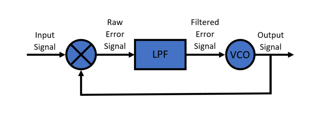
All Analog Phase Lock Loops have three basic components; a Mixer, a Low Pass Filter (LPF) and a Voltage Controlled Oscillator (VCO). The inputs to the Mixer include a reference signal (i/p signal) and a VCO signal (o/p signal). In case these are not phase and frequency synchronized an error signal will be generated which will consist of a sinusoid that has a frequency which is the difference of the two frequencies and a sinusoid that has a frequency which is the sum of the two frequencies. An LPF is then used to remove the high frequency component and the low frequency component is used as a control signal by the VCO. As the name suggests the output of the VCO is a signal whose frequency is directly proportional to the input voltage. Higher the difference between input and output frequency greater is the value of the error signal.
There are three main modes of operation of PLLs.
- Free running: no input is applied
- Capture mode: input is applied and output starts tracking it
- Lock mode: input and output are synchronized in phase and frequency
Type-1 Phase Lock Loop
%%%%%%%%%%%%%%%%%%%%%%%%%%%%%%%%%%%%%%%%%%%%%%%%%%%%%%%%%%%%%%%%%%%%%
% Sampled time-domain simulation of an analog Phase Locked Loop (PLL)
% (Type-1 with Multiplier, Low-Pass Filter and VCO)
%
% Adapted from aaronscher.com
%
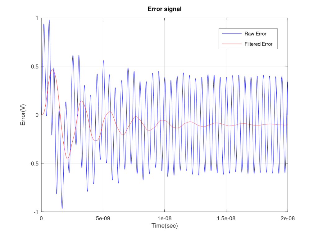
% The input signal or reference signal is a simple sinusoid.
% The output signal is also a sinusoid that tracks the frequency
% of the reference signal after a certain start up time.
%%%%%%%%%%%%%%%%%%%%%%%%%%%%%%%%%%%%%%%%%%%%%%%%%%%%%%%%%%%%%%%%%%%%%
clear all
close all
%Simulatiuon Parameters
N=2000;
fc=1e9;
phase_ref=0.5;
f_VCO=1.1e9;
K_VCO=1.0e9;
fs=100*fc;
filter_length=100;
% Defining the Filter Coefficients
filter_coeff=0.54-0.46*cos(0:2*pi/filter_length:2*pi);
filter_coeff=filter_coeff/sum(filter_coeff);
% Initialiazing the Signal Vectors
ts=1/fs;
t_vec=0:ts:(N-1)*ts;
ref_signal=sin(2*pi*fc*t_vec+phase_ref);
output_phase=zeros(1,N);
output_signal=zeros(1,N);
error_mult=zeros(1,N+filter_length);
% PLL Loop (Multiplier, Filter, VCO)
for n=2:N
t=(n-2)*ts;
error_mult(n+filter_length-1)=ref_signal(n)*output_signal(n-1);
error_filtered(n)=sum(error_mult(n-1:n+filter_length-1).*(filter_coeff));
output_phase(n)=output_phase(n-1)+2*pi*error_filtered(n)*K_VCO*ts;
output_signal(n)=sin(2*pi*f_VCO*t+output_phase(n));
end
%Plot Error Signal
plot(t_vec,error_mult(filter_length+1:end),'b');hold on
plot(t_vec,error_filtered,'r');hold off
title('Error signal')
xlabel('Time(sec)')
ylabel('Error(V)')
legend('Raw Error','Filtered Error')
grid on
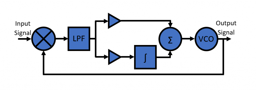
Type-2 Phase Lock Loop
%%%%%%%%%%%%%%%%%%%%%%%%%%%%%%%%%%%%%%%%%%%%%%%%%%%%%%%%%%%%%%%%%%%%%
% Sampled time-domain simulation of an analog Phase Locked Loop (PLL)
% Type-2 with Multiplier, Low-Pass Filter, VCO, Gains and Integrator
%
% Adapted from aaronscher.com
%
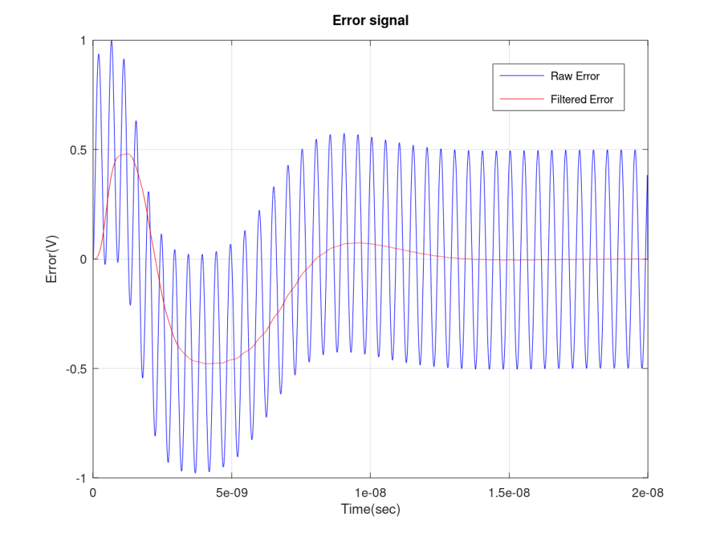
% The input signal or reference signal is a simple sinusoid.
% The output signal is also a sinusoid that tracks the frequency
% of the reference signal after a certain start up time.
%%%%%%%%%%%%%%%%%%%%%%%%%%%%%%%%%%%%%%%%%%%%%%%%%%%%%%%%%%%%%%%%%%%%%
clear all
close all
% Simulation Parameters
N=2000;
fc=1e9;
phase_ref=0.5;
f_VCO=1.1e9;
K_VCO=0.5e9;
fs=100*fc;
filter_length=100;
G1=0.5;
G2=2.0e8;
% Defining the Filter Coefficients
filter_coeff=0.54-0.46*cos(0:2*pi/filter_length:2*pi);
filter_coeff=filter_coeff/sum(filter_coeff);
% Initialiazing the Signal Vectors
ts=1/fs;
t_vec=0:ts:(N-1)*ts;
ref_signal=sin(2*pi*fc*t_vec+phase_ref);
output_phase=zeros(1,N);
output_signal=zeros(1,N);
branch1=zeros(1,N);
branch2=zeros(1,N);
error_mult=zeros(1,N+filter_length);
% PLL Loop (Multiplier, Filter, VCO)
for n=2:N
t=(n-2)*ts;
error_mult(n+filter_length-1)=ref_signal(n)*output_signal(n-1);
error_filtered(n)=sum(error_mult(n-1:n+filter_length-1).*(filter_coeff));
branch1(n)=G1*error_filtered(n);
branch2(n)=branch2(n-1)+G2*error_filtered(n)*ts;
PI_error(n)=branch1(n)+branch2(n);
output_phase(n)=output_phase(n-1)+2*pi*PI_error(n)*K_VCO*ts;
output_signal(n)=sin(2*pi*f_VCO*t+output_phase(n));
end
%Plot Error Signal
plot(t_vec,error_mult(filter_length+1:end),'b');hold on
plot(t_vec,error_filtered,'r');hold off
title('Error signal')
xlabel('Time(sec)')
ylabel('Error(V)')
legend('Raw Error','Filtered Error')
grid on
Type-1 vs Type-2
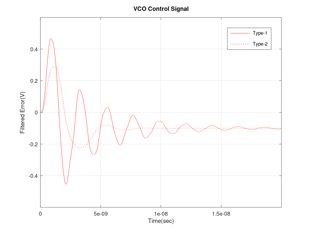
We have seen that the filtered error of Type-2 PLL goes down much more rapidly than Type-1 PLL. But now let us look at the input to the VCO, the control signal to the VCO. This is not the same as LPF output as one more stage is added in Type-2 PLL. But before we do an analysis of the results, we must warn you that a PLL is a non-linear system and the results might not always make sense. Some linear models of PLLs do exist that make the analysis simpler. This will be the subject of a future post.
If we make K_VCO to be the same for both the PLLs (it was not the same in the above examples) than we can make an apple to apple comparison. We set K_VCO to be 1.0e9 for both the cases and then look at the VCO control signal. As expected, the VCO control signal settles down much more quickly in Type-2 than in Type-1. This is the main advantage of Type-2 PLL, it locks on to the reference much more quickly.
Simulation results have shown that capture range of Type-2 PLL is also larger than Type-1 PLL. When the difference in input and output frequency is more than 400MHz the control voltage of Type-1 PLL keeps oscillating and PLL does not go into lock. One might think that reducing the cut-off frequency of the LPF can solve this problem, but this is not the case. According to some references increasing K_VCO and cutoff frequency of the LPF in fact increases the capture range.
To further understand the PLL we need to revisit damped sinusoidal function and its s-domain equivalent. This will be the topic of a future post.
Note:
- A PLL can also be used as an FM demodulator by taking the output of the loop filter before its fed to the VCO.
- It is possible for a PLL to have a phase offset between input and output, but when locked, the output frequency must exactly track the input frequency.
- The type of a PLL refers to the number of poles of the loop transfer function located at the origin. This is controlled by the number of integrators in the loop, VCO being one integrator itself.
- For the filter coefficients we just used a Hamming window since it works quite well and not everyone has access to Signal Processing toolbox which provides the “fir1” function.
- For Digital PLLs the mixer is replaced by a XOR gate, which gives a high output whenever the two digital inputs are different. This signal is then passed on to a simple moving average filter the output of which is used to control the VCO. When the two inputs to the XOR gate are perfectly synchronized in phase and frequency the output of the XOR gate is zero.
References:
http://www.aaronscher.com/phase_locked_loop/matlab_pll.html
https://www.electronics-notes.com/articles/radio/pll-phase-locked-loop/tutorial-primer-basics.php
https://www.analog.com/en/analog-dialogue/articles/phase-locked-loop-pll-fundamentals.html